.svg)
.svg)


Why we invested in Quantum Diamonds
.svg)
.svg)
For decades, progress in semiconductors meant one thing: making transistors smaller. Every generation packed features more tightly into the plane, and the whole industry was built around that axis. AI-driven compute demand is now set to push chip sales to $1.6 trillion p/a by 2030, and governments everywhere are making production and ownership a core priority.
But shrinking is hitting physical and economic limits, and AI companies need next-gen chips faster than lithography can deliver. The next decade will be won not by shrinking but by stacking: advanced packaging, chiplets, 3D architectures, memory stacks like HBM. The energy stakes rise with it, in a sector where fab energy use rose 125% in eight years, and data centre demand is set to triple by 2030, heading for 4% of global electricity.
The old tools were built for the old era
Metrology and inspection are how a fab knows what it has made. The incumbent X-ray, optical and thermal tools were engineered for a flat world: look down at a surface, measure the structures you see, infer performance from geometry. In a 2D era, that logic held, and these instruments became extraordinarily good at it.
Stacking breaks the logic twice over. First, you cannot see through layers, so defects buried within a stack remain hidden. Second, and more fundamentally, structure stops predicting behaviour. A chip’s job is to guide current through complicated shapes and turn that flow into computation. The current is the whole point, and no fab tool measures it directly. Every existing tool is a proxy that used to be good enough, until now.
That blind spot is expensive. Hidden defects cost chipmakers billions every year. The carbon arithmetic runs the same way: a defective chip burns the same manufacturing energy as a functional one, so lost yield is carbon emitted for nothing.
How Quantum Diamonds (QD) built the tool the 3D era needs
QD has built the first commercial chip-testing device based on quantum sensing. Using nitrogen-vacancy centres in diamonds, it images the magnetic fields generated by current flow inside chips. It is a bit like an “X-ray for magnetic fields.” This patented technology allows customers in the semiconductor industry to detect hidden defects in complex 3D chip architectures without destroying the chip.
Crucially, QD combines the resolution of laboratory techniques with the speed industry demands. AI-driven software reconstructs current flow in real time and flags anomalies automatically. Engineers get clear, actionable insights. And there is no destructive sample prep. No vacuum chambers. No delay. For the first time, manufacturers have a tool that can dramatically improve production efficiency and cut waste. It represents a step-change in chip production. One customer had been hunting a defect for six weeks; with QD’s tool they found it in under 60 seconds.
The gap will only widen
The incumbent modalities have been engineered for decades and are close to the end of their levers: any further gains are small and hard-won. QD measures a different quantity entirely, and the physics of measuring it is already solved. Ahead of the company lies a stack of engineering levers, not a hunt for breakthroughs. Measurement time has already gone from a month during research at TU Munich to a minute today, and the remaining levers can take it down to seconds. What stands between today’s lab systems and fab tools at production speed is throughput, automation and reliability at volume.
Why the time is ripe for QD to become the next European chip equipment leader
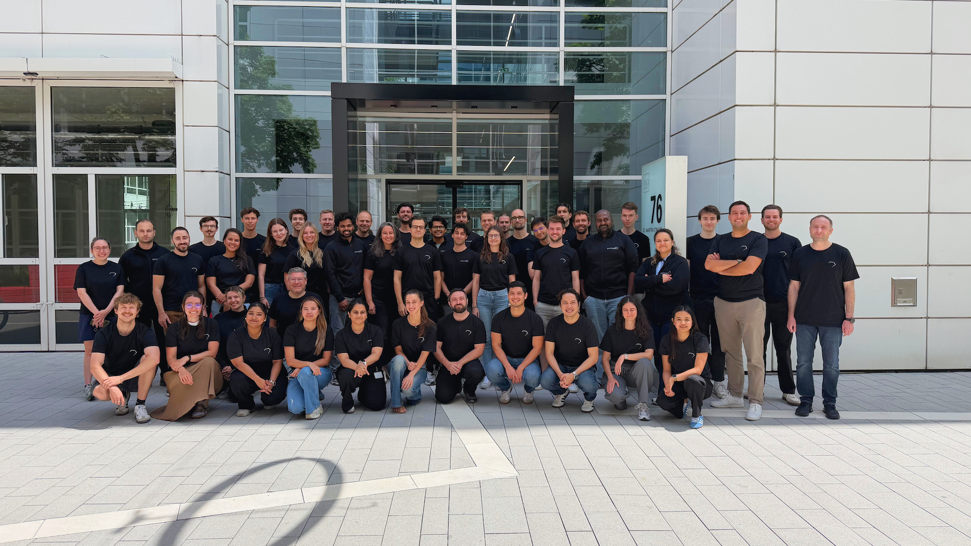
Kevin Berghoff and Dr Fleming Bruckmaier spun QD out of TU Munich in 2022 and have scaled rapidly: 70 people, 18 nationalities, nearly a third with PhDs, pairing quantum-sensing depth with semiconductor veterans. We believe these founders and their impressive, driven, technologically skilled team can become Europe’s next chip equipment champion.
First, their timing is exceptional. The semiconductor testing equipment market is expected to reach $20.4 billion by 2030, and global fab investments are set to exceed $1 trillion by 2030. Most of this is directed at 3D chips for AI, EVs, and high-performance computing. Nearly a third of fab CapEx goes into machinery and equipment. Almost half of that is invested in metrology and inspection.
Second, QD is demonstrating impressive commercial traction. The company is already engaged with 9 of the world’s top 10 semiconductor manufacturers and has deployments live in the US and Taiwan.
This is a company with the potential to become the next global leader in creating the tools that make advanced chips possible. Europe has a history here: ASML in lithography. Zeiss leads optics. Trumpf sets the standard in lasers. These companies each created a unique advantage by leaning into Europe’s strengths in precision engineering and its highly skilled talent pool.
Each category has essentially one name, and every one of those names was settled in the shrinking era. The 3D era needs a fundamentally new approach. QD has the chance to become that name. Kevin and Fleming have assembled a world-class team at the heart of Europe’s strongest semiconductor cluster. Now, the European Chips Act is mobilising €43 billion to secure the region’s role in this industry and has selected QD as one of only two German startups to receive major backing.
World Fund just led QD’s €15 million equity round, which the company raised alongside €76 million in non-dilutive funding from the ECA. QD will use this funding to scale production at its new €152 million production facility in Munich, deliver lab systems to leading chipmakers, and advance wafer-level capabilities for high-throughput fab inspection. The company will also double its engineering team over the next 12 months and work to give Europe a commercial and technological lead in a cutting-edge inspection capability.
QD is exactly the kind of company Europe needs to build: frontier technology, born from deep science, scaling into a strategic global market. We can't wait to support Kevin, Fleming and his talented team as they go global with their transformative technology.
If you have any questions or would like to discuss further, please get in touch with Robin at robin@worldfund.vc.

.JPG)
.avif)


.svg)
.svg)
.svg)